
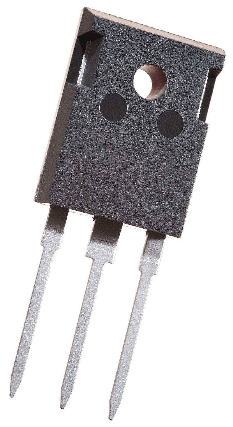
The new large-die device, which hits 90 mΩ on-resistance and 55 A drain current, is currently sampling to U.S. customers. By leveraging a junction-barrier Schottky FET (JBSFET) construction, the design aims to mitigate body diode degradation, a common failure point in high-stress environments. These components are intended for heavy-duty applications, including rail traction, MW-scale EV charging, and solid-state transformers.
Dr. Adam Morgan, CEO of NoMIS Power, noted that the successful scaling from the company’s existing 3.3 kV line to this high-voltage class establishes a domestic supply chain for sectors like aerospace and defense. With standard production for the 6.5 kV line slated for Q4 2026, the company is positioning itself as a secure alternative to foreign single-source dependencies. Operating out of the Albany Nanotech Complex, NoMIS Power is currently engaging developers to integrate these high-voltage solutions into government-funded programs, with plans to push their architecture toward the 20 kV threshold in the coming years.
Comments (0)
No comments yet. Be the first!